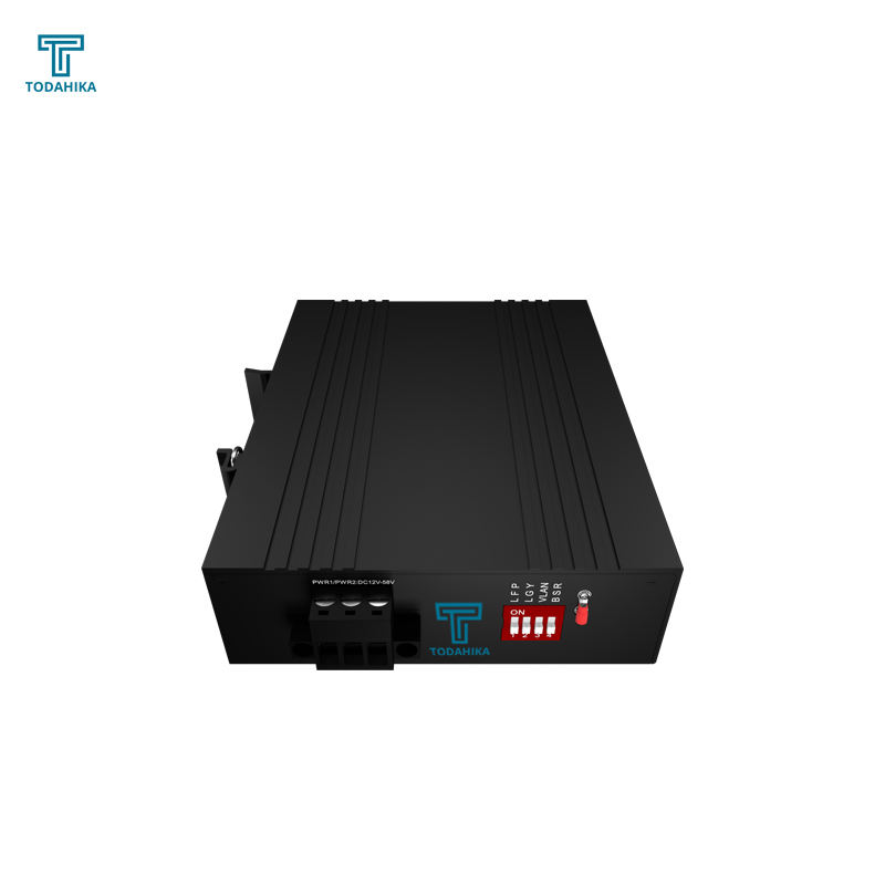
Network switches are the backbone of modern communications networks, ensuring seamless data flow between devices in enterprise and industrial environments. The production of these vital components involves a complex and meticulous process that combines cutting-edge technology, precision engineering and strict quality control to deliver reliable, high-performance equipment. Here’s a behind-the-scenes look at the manufacturing process of a network switch.
1. Design and development
The manufacturing journey of a network switch begins with the design and development phase. Engineers and designers work together to create detailed specifications and blueprints based on market needs, technological advancements and customer requirements. This stage includes:
Circuit design: Engineers design circuits, including the printed circuit board (PCB) that serves as the backbone of the switch.
Component selection: Choose high-quality components, such as processors, memory chips, and power supplies, that meet the performance and durability standards required for network switches.
Prototyping: Prototypes are developed to test the functionality, performance, and reliability of a design. The prototype underwent rigorous testing to identify any design flaws or areas for improvement.
2. PCB production
Once the design is complete, the manufacturing process moves into the PCB fabrication stage. PCBs are key components that house electronic circuits and provide the physical structure for network switches. The production process includes:
Layering: Applying multiple layers of conductive copper to a non-conductive substrate creates electrical paths connecting various components.
Etching: Removing unnecessary copper from a board, leaving the precise circuit pattern required for switch operation.
Drilling and Plating: Drill holes into the PCB to facilitate placement of components. These holes are then plated with conductive material to ensure proper electrical connection.
Solder Mask Application: Apply a protective solder mask to the PCB to prevent short circuits and protect the circuitry from environmental damage.
Silk Screen Printing: Labels and identifiers are printed on the PCB to guide assembly and troubleshooting.
3. Parts assembly
Once the PCB is ready, the next step is to assemble the components onto the board. This stage involves:
Surface Mount Technology (SMT): Using automated machines to place components onto the PCB surface with extreme precision. SMT is the preferred method for connecting small, complex components such as resistors, capacitors, and integrated circuits.
Through-Hole Technology (THT): For larger components that require additional mechanical support, through-hole components are inserted into pre-drilled holes and soldered to the PCB.
Reflow soldering: The assembled PCB passes through a reflow oven where the solder paste melts and solidifies, creating a secure electrical connection between the components and the PCB.
4. Firmware programming
Once the physical assembly is complete, the network switch’s firmware is programmed. Firmware is the software that controls the operation and functionality of hardware. This step includes:
Firmware installation: Firmware is installed into the switch’s memory, allowing it to perform basic tasks such as packet switching, routing, and network management.
Testing and Calibration: The switch is tested to ensure the firmware is installed correctly and all functions are functioning as expected. This step may include stress testing to verify switch performance under varying network loads.
5. Quality Control and Testing
Quality control is a critical part of the manufacturing process, ensuring each network switch meets the highest standards of performance, reliability and security. This stage involves:
Functional Testing: Each switch is tested to ensure it is functioning properly and that all ports and features are functioning as expected.
Environmental testing: Switches are tested for temperature, humidity, and vibration to ensure they can withstand a variety of operating environments.
EMI/EMC Testing: Electromagnetic interference (EMI) and electromagnetic compatibility (EMC) testing is performed to ensure that the switch does not emit harmful radiation and can operate with other electronic devices without interference.
Burn-in testing: The switch is powered on and run for an extended period of time to identify any potential defects or failures that may occur over time.
6. Final assembly and packaging
After passing all quality control tests, the network switch enters the final assembly and packaging stage. This includes:
Enclosure Assembly: The PCB and components are mounted within a durable enclosure designed to protect the switch from physical damage and environmental factors.
Labeling: Each switch is labeled with product information, serial number, and regulatory compliance marking.
Packaging: The switch is carefully packaged to provide protection during shipping and storage. The package may also include a user manual, power supply, and other accessories.
7. Shipping and Distribution
Once packaged, the network switch is ready for shipping and distribution. They are sent to warehouses, distributors or directly to customers around the world. The logistics team ensures that the switches are delivered safely, on time, and ready for deployment in a variety of network environments.
in conclusion
The production of network switches is a complex process that combines advanced technology, skilled craftsmanship and strict quality assurance. Every step from design and PCB manufacturing to assembly, testing and packaging is critical to delivering products that meet the high demands of today’s network infrastructure. As the backbone of modern communications networks, these switches play a vital role in ensuring reliable and efficient data flow across industries and applications.
Post time: Aug-23-2024


